Table Of Content

SparkFun Electronics[23] is a company that has grown due to the hobbyist market exemplified by Make magazine and others. Many of these companies offer EAGLE part libraries[24] which define schematic shapes, pinouts, and part sizes to allow for correct layout in the PCB layout editor. EAGLE provides a multi-window graphical user interface and menu system for editing, project management and to customize the interface and design parameters.
PCB Design and Layout Services
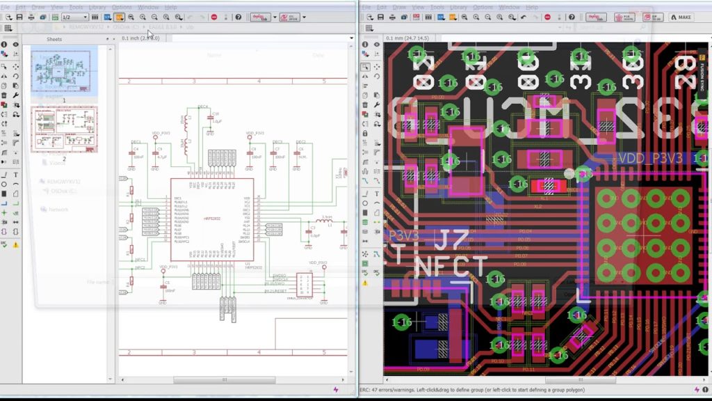
The schematic editor (on the left above) is a collection of red circuit symbols which are interconnected with green nets (or wires). A project's schematic is like the comments in a program's code. It helps tell the story of what the board design actually does, but it doesn't have much influence on the end product. When you've finalized your design, the last step before sending it off to the fab house is to generate gerber files. Gerber files are kind of a "universal language" for PCB designs.
Layout Specializations
We select components, design schematics and PCB layouts, and create one or more prototypes. The team identifies and eliminates bugs, and optimizes the performance of the devices. Components are added to the schematic in symbolic form, and at this stage, they are placed randomly without any connections between them. In the case of a simple circuit like this, where you have a small number of components, it’s manageable. However, in real-world scenarios with numerous components, you should have a layout in mind to position the components logically and prevent crossovers when connecting them.
Download, Install, Run
After placing a part, the add tool will assume you want to add another -- a new frame should start following your cursor. To get out of the add-mode either hit escape (ESC) twice or just select a different tool. Give the newly created, red project folder a descriptive name. It can be hard to tell what is and isn't connected to the ground pour.
EAGLE version 7.2
This button is used to switch between schematic and board layout windows. Once your board design is complete your board layout would look something like this below. If you wish to adjust the routing style, right-click to modify the route’s bend style. By default, for through-hole components, the bottom layer serves as the trace layer. You can switch this to the top layer with a center-click or through the drop-down menu.
Board Support Package (BSP) Development
The customer will receive all the necessary instructions on how to use the product. We will also answer any questions and provide training if necessary. Getting Autodesk EAGLE up and running on Windows, Mac, or Linux is as easy as can be.
PCB Design Review: ESP32-S3 Round LCD Board - Hackaday
PCB Design Review: ESP32-S3 Round LCD Board.
Posted: Tue, 19 Mar 2024 07:00:00 GMT [source]
Download the software and install it by following simple on-screen instructions. After installation, launch the software and you will be greeted with the dialog box below. Whichever manufacturer you pick, there will be an option to preview your Gerber file before you place your order. This will allow you to see what the manufacturer will see in order to ensure everything is correct.
Hence is important for every engineer to learn PCB designing to design their own PCB boards for their circuits and applications. The image above is an image of the fully routed PCB I created for the Dice Generator project. Routing can be done using the 'route' tool on the left control panel. If you are planning to route on more than one layer, you can interchange between these layers using the 'layer' drop-down menu above. The process of sending gerber files varies by fab house. Most will ask you to send them a zipped folder of select files.

With EAGLE’s online Forward- and Back annotation you can simply select the schematic window, add the capacitor and connect it. Simultaneously, you can see the part and signals being added to the board window. And it is just as easy to swap pins and gates, change names or draw additional connections. And as always, any editing function you use can be 100% undone thanks to EAGLE’s outstanding Undo/Redo function. Simply pick up an air wire, adjust the angle with the right mouse button, and select the layer with the center button. Our PCB layout design specialists have decades of experience delivering printed circuit boards with industry-leading quality for both start-ups & Fortune 500 companies alike.
We use Altium Designer, Eagle Cad, Cadence Allegro, OrCad, and KiCad. All these programs have enhanced features for building both simple and the most complex boards. We have a large, trusted library of components for each of these CADs. If you give preference to a certain program or tool, you are welcome to choose and advise. We are flexible and ready to discuss every detail before development starts. Upon project completion, the customer receives a fully functional PCB, detailed technical documentation, the source code of the firmware, and PCB design files in a CAD format.
Copper pours are usually a great addition to a board. They look professional and they actually have a good reason for existing. Usually, when you're adding a copper pour it's for the ground signal. If ratsnest says you have "N airwires" left to route, double check your board for any floating golden lines and route them up. If you've looked all over, and can't find the suspect airwire, try turning off every layer except 19 Unrouted. The new board file should show all of the parts from your schematic.
Public hearing on PCB landfill design plan rescheduled for April 18 at Lee Middle and High School - Berkshire Eagle
Public hearing on PCB landfill design plan rescheduled for April 18 at Lee Middle and High School.
Posted: Fri, 05 Apr 2024 07:00:00 GMT [source]
We always set realistic deadlines when preparing the spec and stick to the schedule at all project stages. I believe this has sparked enough interest to start with our tutorial series. In the next part we will learn more about schematics editor and how to use in to create your own schematics on Eagle. Modify the dimensions of the outline box by using the MOVE command on the corners or by right-clicking on a segment.
We can also prepare manuals if the product is designed for in-house use. In parallel with hardware development or right after that, the team starts creating the firmware for the board. When the electronic circuit design is finished, we reveal and eliminate bugs and optimize the performance of the firmware. At the time of writing this article, the latest version of software is 9.4.2, but you can also download latest software that is available at your time. Since most of the basic features will still remain the same, you can still follow the same tutorial. The link given will take you to a page where you have downloaded the suitable software based on your Operating system.
Learn how to access and design using your next electronic design using Autodesk Fusion. Autodesk Fusion offers a complete online experience for PCB, mechanical and data management, ensuring every stakeholder is part of the product development cycle. Autodesk Fusion enables ECAD and MCAD designers to work independently and natively on the same project and within the same design management platform. Product design and manufacturing requires end-to-end solutions, not electronic point solutions. Autodesk Fusion is a unified product development solution that integrates design, simulation, electronics, manufacturing, collaboration and more. EAGLE is available only with a Autodesk Fusion subscription.
Launch the software and locate the ‘File’ button in the top menu bar. From the dropdown options, select ‘New’ and ‘Schematic’ to create a new project. Next, we'll use the NAME tool -- (left toolbar, or under the Edit menu) -- to name each of the six nets.


No comments:
Post a Comment